This ChipRack project update indicates that the replacement of the custom designed PCB with a multi-purpose multi-product intelligent communications framework could substantially cut manufacturing costs and generate major society and consumer benefits.
Key Proposals
- It is possible to design an intelligent two or three dimensional communications framework which would allow ICs, sub-assemblies and modules to be attached and then to identify each other and to configure themselves into a functional product. Software would sculpt the product.
- Communication between ICs, sub-assemblies and modules internally and externally with other devices could now largely be achieved by means of high speed electrical, wireless or multi-spectral optical serial communication.
- If we refocus our attention from specific electronic products onto an intelligent modular communications framework to replace the traditional PCB we can consider the opportunity for a new marketable item to be a multi-purpose multi-product intelligent communications framework.
- Replacement of the custom designed PCB with a multipurpose communications framework could substantially cut cost and enable simplified production methods.
- There would be major society and consumer benefits — it would facilitate upgrade, repair and re-designation; reuse of functional electronic blocks; an eco-friendly route to reduce the mountain of electronics waste.
Background: The Original Chiprack Project
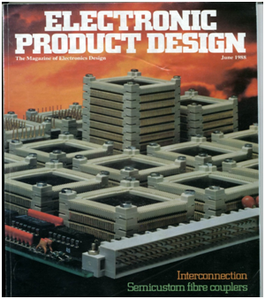
Around 30 years ago there was an unusual project involving Dowty, Inmos, Cambridge University and a range of other players which became known as 'Chiprack'. It sparked considerable excitement at the time when it won a number of awards and so it seemed timely to have another look.
Chiprack was, in essence, a modular two or three dimensional communications framework for supporting and interconnecting arrays of large scale circuits or modules. One of its objectives was to facilitate the recycling and reuse of electronic sub-assemblies (as functional electronic units).
At that time this was ultimately seen as commercially undesirable — rapid obsolescence was seen as a route to maximising profit growth. Times change, and with mounds of electronic waste starting to cause concern it may be useful to revisit this problem.
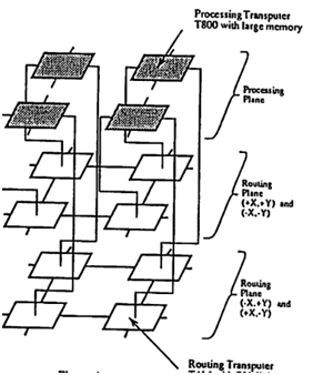
One of the Chiprack prototypes that generated most interest involved a three-dimensional array of Transputers (in the heady days of Inmos, the British semiconductor manufacturer!). The Transputers were coupled into three-dimensional arrays using the Chiprack mechanical structures and they then communicated using high speed serial Transputer links. At the same time a team at Bristol University demonstrated the use of high speed optical links to link Chiprack precision-aligned mounted sub-assemblies — different frequencies of light generating a span of communication channels.
What's New Now?
What may be new and useful, in the light of the Chiprack project, may be to consider how some of these ideas may be combined and then usefully designed into future products. Products have traditionally been considered as independent functional electronic units that connect onto a range of communications networks. Perhaps we could refocus our attention onto the communications framework and consider the opportunity for the new marketable item to be an intelligent communications framework — onto which functional, add-on, replaceable electronic modules could be mounted, identified by the framework, and then sculpted into product functionality.
References
Parallelogram Mar 88, 'Transputer Sandwiches' — Original Chiprack video clip
EUPAC '94 7th International Conference, Essen, Germany — 'Chiprack Project: A Report on Progress'
INTERNATIONAL CONFERENCE ON ASIC, Beijing, China, 1994 — 'A Novel Approach to the Problem of Partitioning Highly Integrated VLSI Systems'
http://www2.eng.cam.ac.uk/~dmh/chiprack/chiprack.html
INTERNATIONAL CONFERENCE ON CLEAN ELECTRONICS, Edinburgh, 9–11 Oct 1995 — 'A Novel Architecture to Facilitate Disassembly and Reuse of Electronic Components and Sub-Assemblies'
Dowty Heritage Web Site: dowtyheritage.org.uk